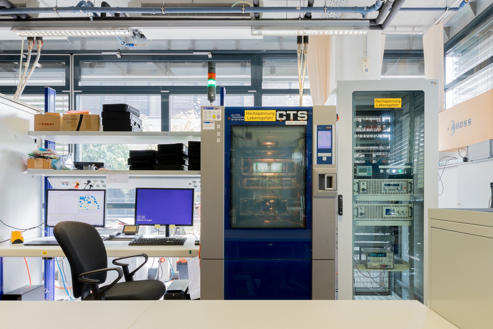
Device & System Reliability Test Concepts
Together, we develop solutions which optimize the reliability and functionality of our customers’ products.
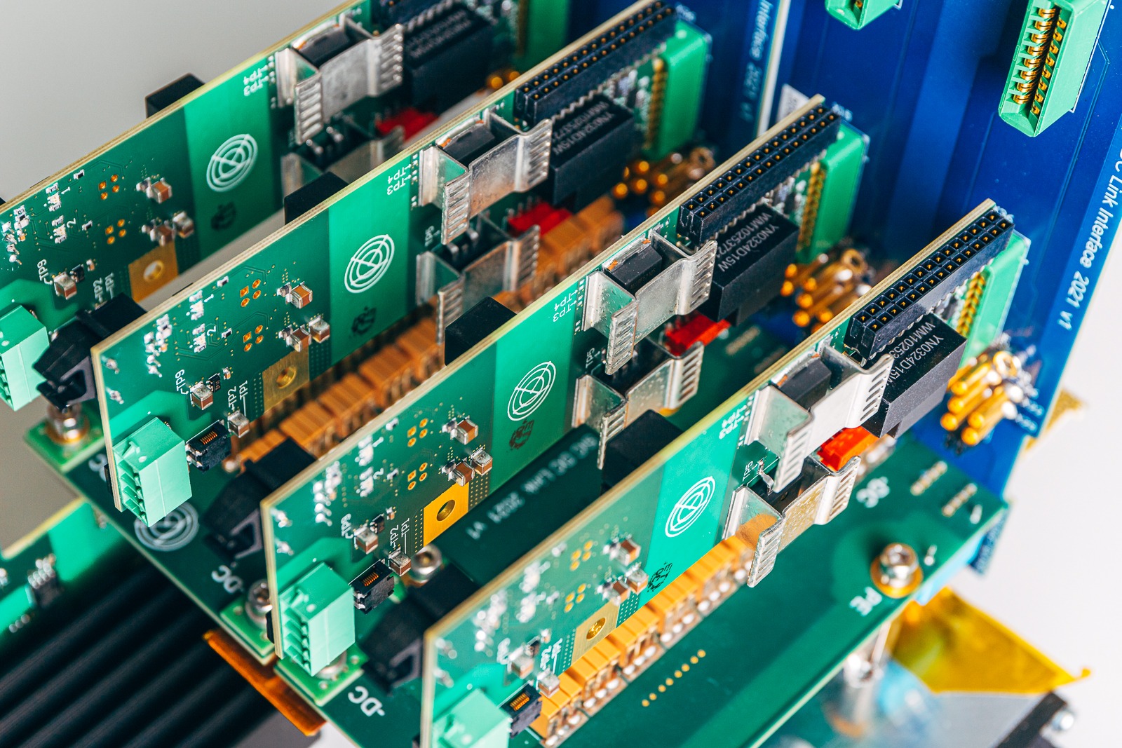
The reliability of semiconductor power devices and systems needs to be investigated during their design process, as well as in the qualification of final products before market release. Comprehensive life test procedures have been described in automotive and industrial standards, but future technologies require new developments in test methodology, such as:
- High power, multi-channel stress test environments for discrete and integrated power devices to cover regular as well as irregular operating conditions (e.g. power cycling, avalanche, short circuit).
- Quick and reliable overload protection to avoid damage to the test equipment in case of catastrophic device failure and retain failed samples for further physical inspection.
- Flexible embedded real-time control of test equipment, driven by a user-programmable distributed state machine environment, to enable cyclic stress testing under variable load conditions.
- Advanced condition monitoring based on in-situ data acquisition and live diagnosis of power device and system state, to detect and record individual stress-related degradation or failure events.
- Application related system level stress test environments (e.g. DC/AC power converter stages) to study robustness and reliability of power devices under real life conditions.
Introduction / Research Goals
Application-relevant stress testing on device and system level is driven by complex technology, design, and customer requirements, motivating our joint research effort at KAI to provide the next generation of test concepts for power devices:
- Dynamic pulse testing of discrete power semiconductors (IGBT, MOSFET, …) at high voltage and current levels (1200 V, 100 A … 300 A) in relevant numbers (up to 100 parallel channels) for statistical significance and valid product qualification.
- Distributed real-time test control for multichannel stress test systems, based on a network of smart sensor and controller nodes linked to a flexible, user-programmable host via a high-speed bus interface.
- Application-oriented stress test concepts for novel power semiconductor technologies, expanding current test system architectures and capabilities to highest switching speeds and MHz frequencies under hard and soft commutation conditions.
- High speed real-time data acquisition and processing concepts to match the fast monitoring and control requirements of dynamic power converter architectures for advanced application stress testing.
- Optimization of electrical and thermal performance of novel stress test concepts by FEM simulation of parasitic impedances and critical cooling conditions.
Competences
Innovative solutions for power semiconductor stress testing
Meeting the requirements for testing and investigating the reliability of the next generation power semiconductors demands innovative solutions. At KAI we develop stress test concepts that meet our customers’ needs, to enable safe and economical operation in industrial laboratory environments with advanced protection features. Thereby, degradation mechanisms and failure patterns can be investigated under accelerated application-level conditions. Whether for voltages up to 2 kV or currents up 1 kA the focus is to enable investigations that help to validate tomorrow’s robustness and reliability requirements of our next generation power semiconductors.
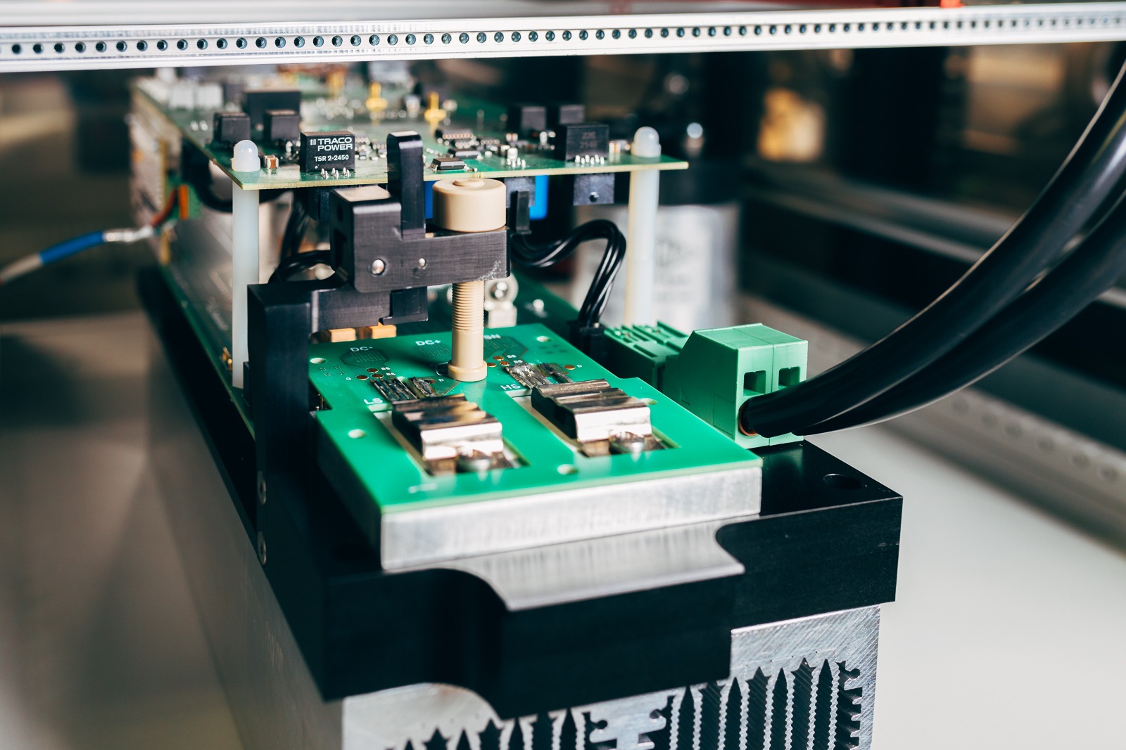
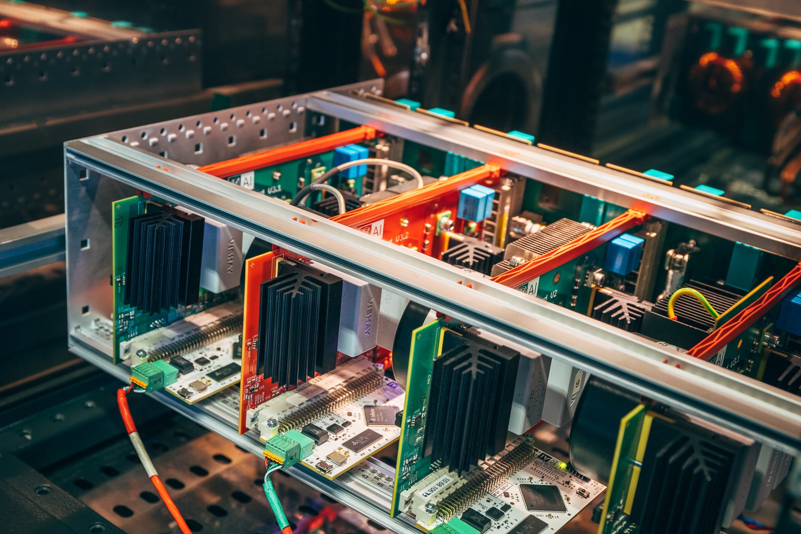
Parallel test systems
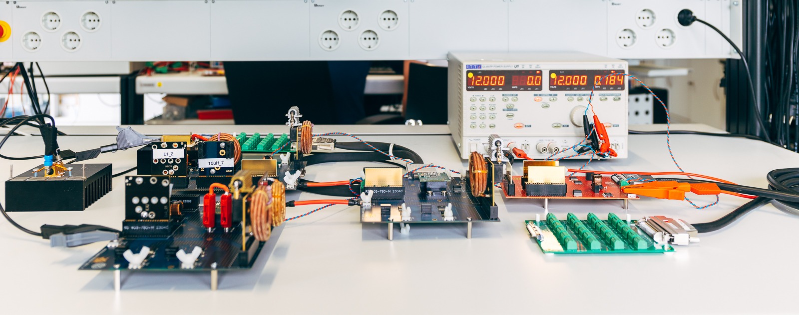
Reliability and robustness validation tests require a certain number of devices under test to deliver statistically relevant conclusions. There are numerous degradation and failure mechanisms that affect power semiconductors during their lifetime. These occur with a certain probability and at a certain stochastic rate. Therefore, it is essential during reliability and robustness validation throughout the development process of new power semiconductor technologies and products to test a statistically relevant number of devices. One of the key competences at KAI is to design and implement multi-channel test systems, thereby enabling the testing of many devices in parallel.
While the fundamental modules are designed to be as simple as possible, to focus on specific degradation and fault mechanisms, the system integration of multiple parallel operating modules brings about many challenges of quite different nature. Low voltage and high current test systems have a focus on peak current carrying capability, whereas high voltage tests (up to 2 kV) must consider the necessary isolation and safety requirements when packing as many modules as possible into a test system. For examples of such test systems, please have a look on our subpages.

Test Control
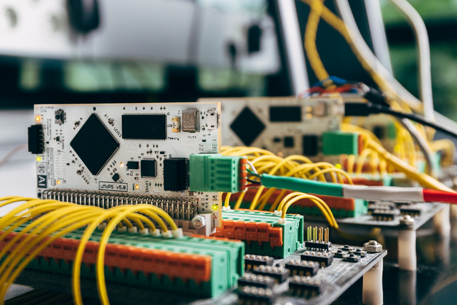
Digital control of power electronic stress test systems requires special attention to facilitate parallelized tests with vastly different operational requirements. At KAI dedicated software and firmware solutions are being developed and deployed to handle a variety of cases. Modular hardware and software concepts significantly reduce the number of development cycles and utilize the available resources as best as possible. A custom designed high-performance 32-bit microcontroller platform that can withstand ambient temperatures from -40°C to beyond 100 °C is just one example.
Our modular power stress platform and our modular software architecture allow a flexible test development, as they have been designed to cater to the different test requirements in application relevant testing of power semiconductors. With the help of finite state machines and a scripting language with an easy-to-use API the test development is significantly simplified for our customers’ test engineers.
System Level Investigations
The next generation power semiconductors strife to reach the optimum performance for their target application. To link the target application’s reliability and robustness requirements to test conditions applied to next generation power semiconductors at KAI we create digital models and hardware demonstrators to investigate first the stress that these applications impose onto next generation power semiconductors. Based on the knowledge gained from such investigations we then develop with our partners the concepts to apply an accelerated form of this stress to the power semiconductor currently being developed.
One example of such system level investigations is the research conducted into replacing conventional relays and fuses with semiconductor solutions in vehicles. Dedicated, digitally adjustable protection features allow a significant copper reduction in the vehicle’s power distribution network as well as error analysis. To investigate potential problems, fault propagation and to identify potentials for optimization at KAI, we have created a representative model and hardware of a wiring harness that is used for researching the behavior of next generation power semiconductors for relay and fuse replacement under various operating conditions and power distribution network architectures.
Virtual prototyping
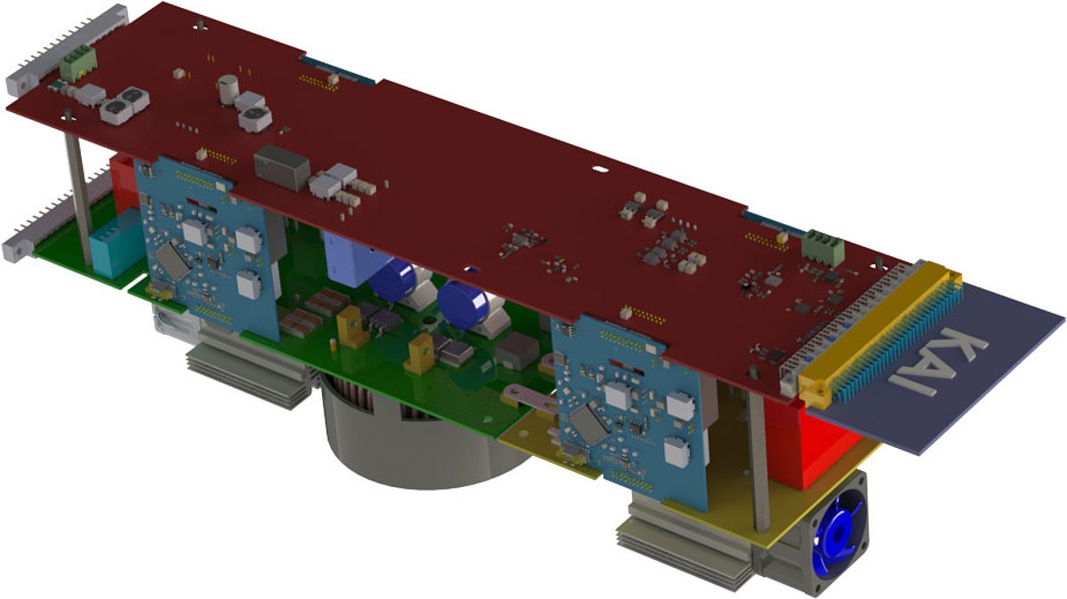
Creating hardware demonstrators is a costly and time consuming task. Therefore, all KAI test system concepts are first studied thoroughly with simulations. With the aid of tools like MATLAB/Simulink, PLECS and SPICE simulation the behavior of potential circuit solutions is investigated. 3D models of printed circuit boards and mechanical components are essential for building parallelized test systems with a high channel count. The adjacent image shows a 3D model of a test module used for evaluating next generation SiC MOSFETs under various operating conditions.
Rapid prototyping / Hardware-in-the-Loop testing
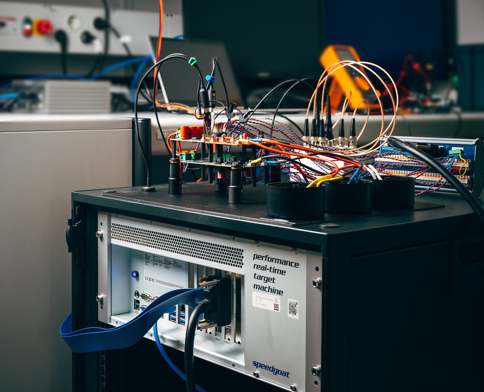
Reducing the time from an idea to a prototype and repeating the cycle to investigate different concepts is essential in today’s economic environment. With the help of rapid controller prototyping platforms, like PLECS RT Box or Speedgoat, we have the ability to validate our simulation concepts with demonstrators without changing the development environment. The power controllers integrated in such systems enable us to connect our digital concepts to hardware quickly and prototype ideas with a minimum effort. Thereby, the feasibility of controller concepts can be tested before developing dedicated hardware. This reduces the possible failure potential, saves valuable development time, and resources which helps to make the development process more sustainable.
Temperature Control of Devices Under Test
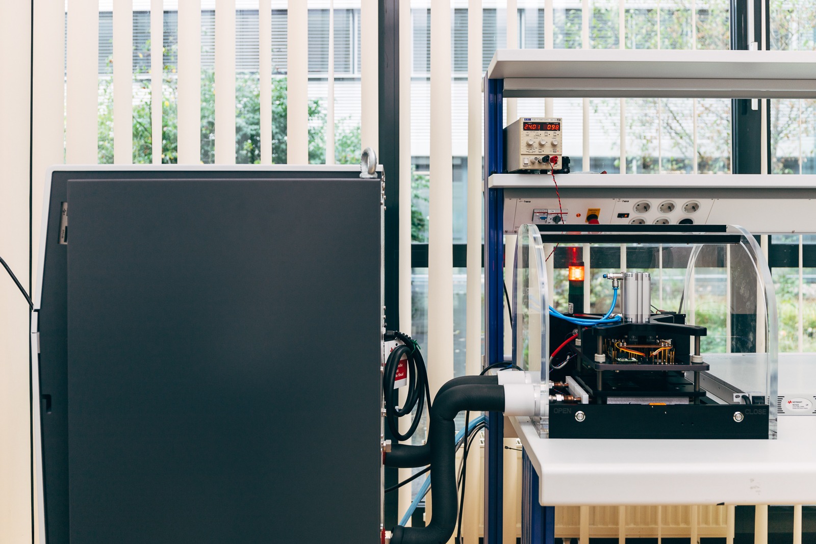
Temperature is one of the most important parameters when investigating the reliability and robustness of power semiconductors. It can serve as an accelerated stress or as a means to operate at controlled conditions. Either case is important when investigating the capabilities of next generation power semiconductors. At KAI we have the ability to use climatic chambers as well as systems with liquid temperature control. This enables us to operate at the relevant temperature and climatic conditions necessary for reliability and robustness validation tests under application conditions.
