Semiconductor Device Physics Laboratory
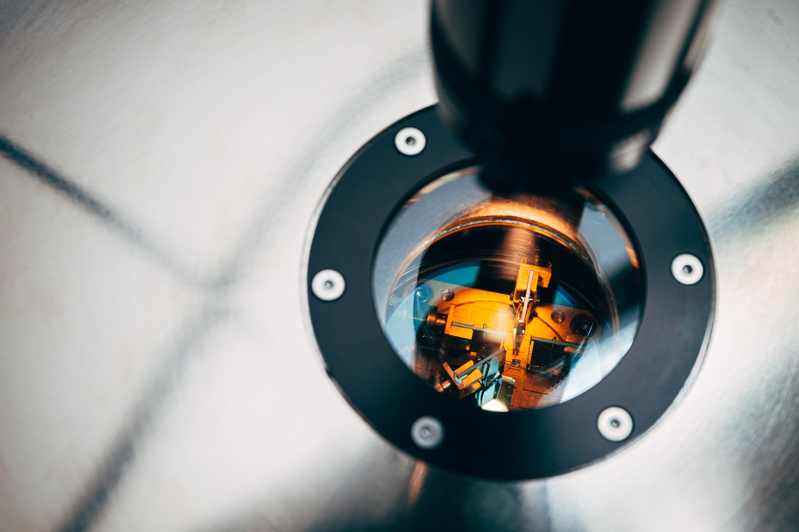
Measurements performed at the KAI device physics laboratory (KAI DPH lab) are conducted to investigate crystal defects in semiconductor devices that can limit their performance and reliability. To this end, the lab is equipped with three probe stations that allow for electrical measurements of semiconductor devices such as diodes or MOSFETs. The device characterization can be done on a single device or on wafer level. The measurements can be performed at temperatures ranging from 6.5K to 473K (-267°C to 200°C). To control the desired measurement sequences, an in-house built LabVIEW software is used, which takes care of all connected instruments and eases the experiment design.
Below, we provide an overview of the measurement equipment available in the KAI DPH lab.
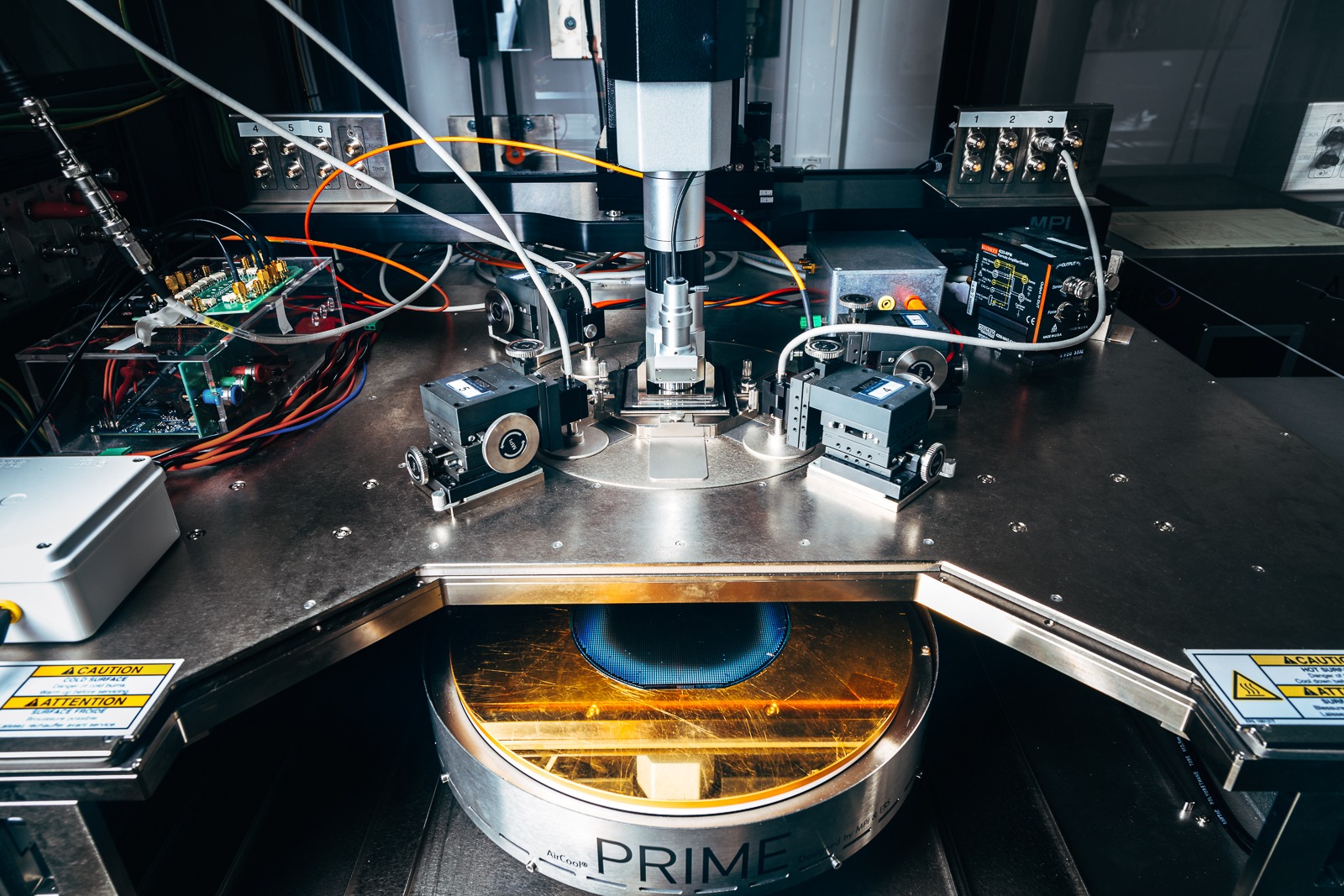
Semi-automatic Probe Station
The semi-automatic probe station is used to perform electrical measurements on devices located on a wafer in a temperature range between -60°C and 200°C. As an additional feature, the chuck is motorized, allowing for automated measurements over the entire wafer. The wafer is placed on the chuck within the probe station, and electrical connections are established via the force/sense needles. To prevent condensation of water and ice on the wafer, the system can be flooded with dry air.
Technical description
At the MPI TS3000 HP semi-automatic probe station many different electrical measurements can be performed. The station’s two switching matrices manage the connections between the Source Measurement Units (SMUs) and the needles, enabling force/sense measurements. To ensure safe measurements with the High-Voltage SMU (HVSMU), a protection unit is required. The HVSMU is capable of measuring up to 1.5kV with 120mA current or up to 3kV with 20mA. The station also includes an impedance analyzer, which allows voltage-dependent capacitance measurement over a frequency range of 20Hz to 2MHz. In addition, a custom-designed multi-channel high-voltage pulse measurement setup can be used at the probe station. The setup includes a needle card PCB with several components (gate driver, clamping circuit, etc.), and a field-programmable gate array (FPGA) for flexible programming of pulse pattern sequences. With this setup, drift effects of test transistors can be measured with oscilloscopes in the range of microseconds to kiloseconds.

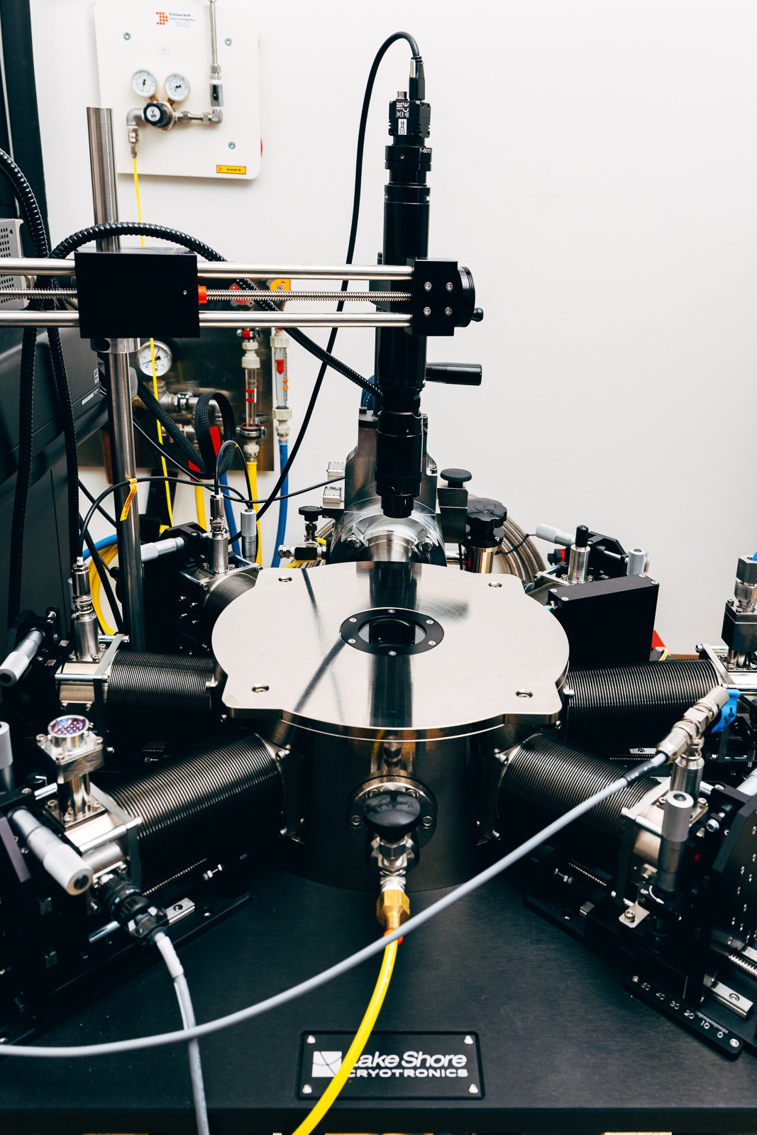
Cryogenic Probe Station
The cryogenic probe station and its electrical measurement equipment enable detailed electrical characterization of single semiconductor devices across a very broad temperature range of 6.5K (-267°C) to 400K (127°C). By using the cryogenic probe station, it is possible to take advantage of the temperature activation of point defect creation/passivation and charging/discharging mechanisms. Cooler temperatures enable the characterization of processes that are too fast for electrical measurements at room temperatures. Additionally, increased temperatures accelerate degradation mechanisms that would normally occur over the course of a few years, reducing them to an acceptable test time of a few minutes or hours. The probe station also includes an optic fiber that allows light from outside of the probe station to be transmitted to the device, enabling the investigation of the interaction between defects in semiconductor devices and light. This feature allows for not only electrical activation and measurement of defects, but also the study of their optical properties.
In addition, the probe station includes a superconductor that can produce an vertical magnetic field of up to 2.5 Tesla. This setup enables Hall measurements over a wide temperature range of 6.5K to 300K.
Technical description
The LakeShore CRX-VF Probe Station is a closed-cycle refrigerator that utilizes liquid helium to perform electrical measurements at temperatures ranging from 6.5K to 400K. The sample chamber is evacuated to a high vacuum of approximately 1e-6 mbar pressure using a turbomolecular vacuum pump. The electrical measurement equipment includes a digital lock-in amplifier with a transimpedance pre-amplifier and an arbitrary waveform generator. These instruments enable the measurement of capacitance transients with a resolution of 10µs and a bias range of +/-10V. As a result, transient measurements of deep levels in semiconductors can be conducted to identify and characterize performance and reliability limiting defects in wide band gap devices. In addition to these features, the cryogenic probe station can be utilized to perform Hall-measurements by applying a magnetic field.
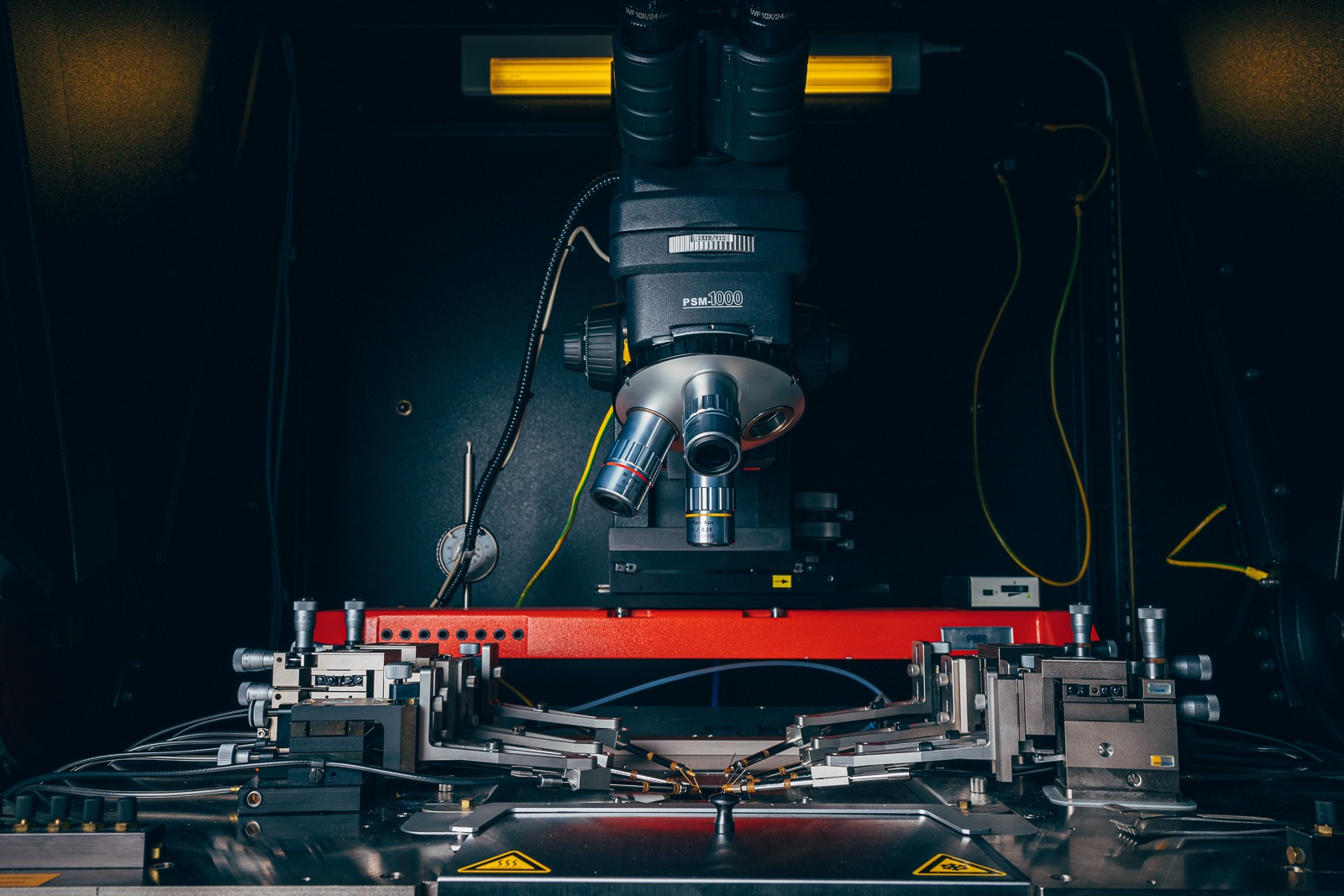
Manual Probe Station for Wafer-level Characterization
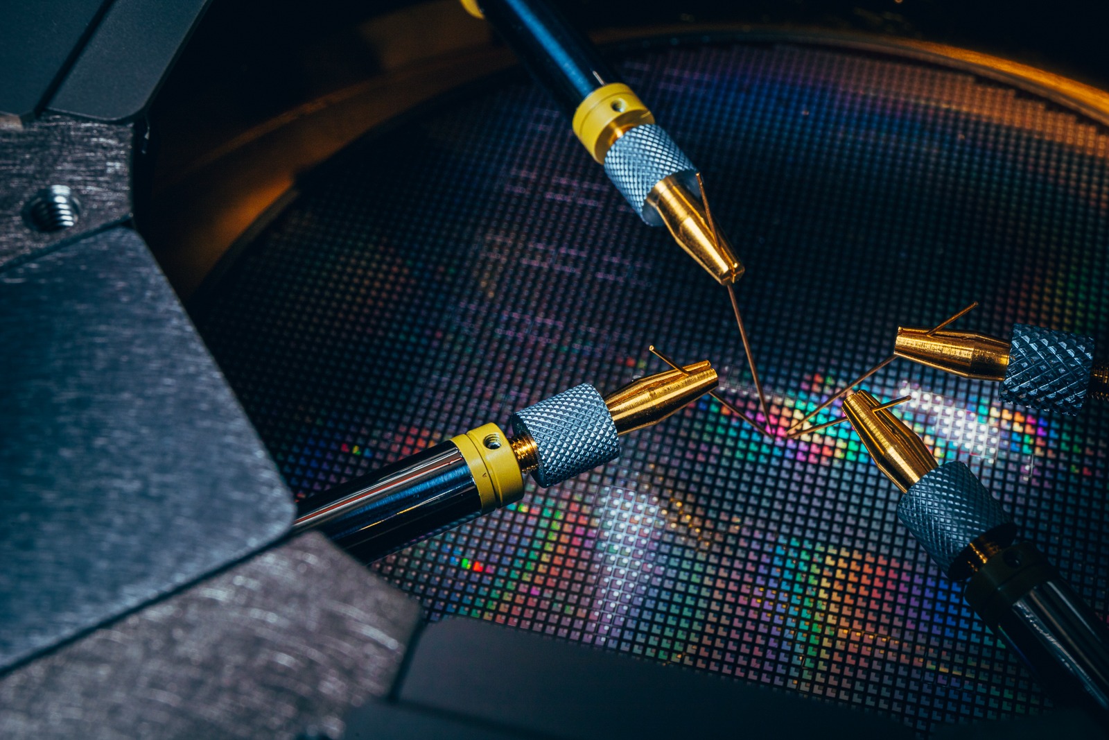
The manual probe station and its electrical measurement equipment enable electrical characterization of individual devices directly on the wafer, eliminating the need to package a device prior to electrical measurement. We use tungsten needles with gold coating alongside probe positioners equipped with micrometer screws to make contact with the device pads on the wafer. The prober features eight individual probe positioners, providing us the ability to contact various different test structures to test them electrically. The wafer lies on an eight-inch chuck, which can be contacted electrically. Its temperature can be varied between -60°C and 200°C. To prevent condensation and ice formation on the wafer, the entire system is flooded with dry air that has a dew point below -70°C.
Technical description
The Süss PM-8-IS Prober’s electrical characterization equipment includes a parameter analyzer, an impedance analyzer, a switching matrix, and a high-voltage unit with an appropriate voltage protection and limiter unit. The parameter analyzer features four medium-power source-measurement-units with maximum voltage/current ranges of 100V/100mA , as well as a high-power unit with voltage/current ranges of 200V/1A . These instruments enable time-resolved current measurements with a delay of approximately 100µs. Additionally, the parameter analyzer includes two pulse-generator-units with an output range of 40V/400mA and a frequency range of 0.1Hz to 33MHz. The high-voltage unit allows for measurements up to 1kV/120mA with a time resolution of 1µs. Electrical measurements can be reliably performed down to the picoampere range. Moreover, voltage-dependent capacitance measurements in the Femtofarad range can be conducted with a frequency range between 40Hz and 1MHz.

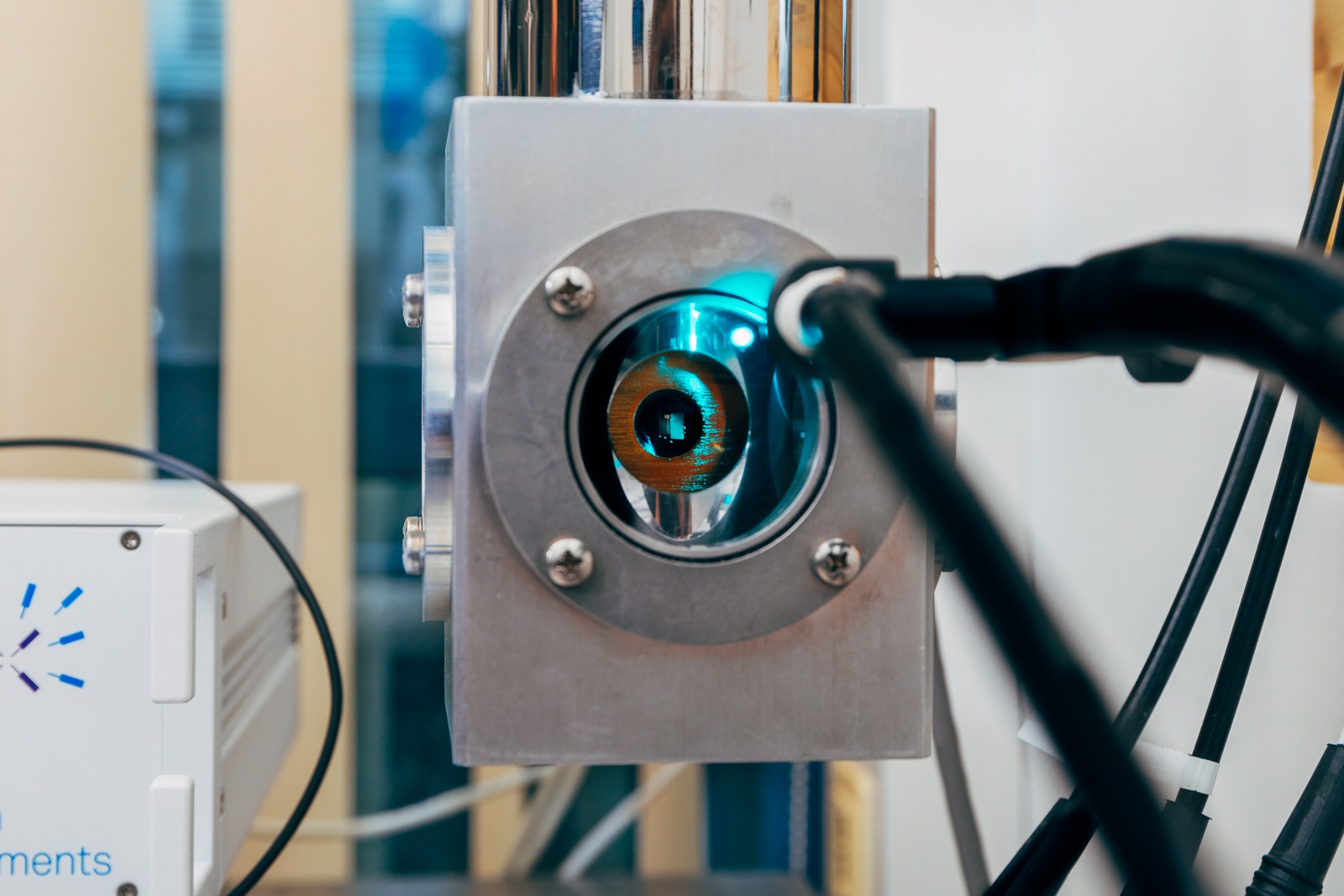
Optical cryostat
This cryostat is specifically designed to provide optical access to the device from all sides. Typically, either the front side or the backside of a device is illuminated via a light guide and a condenser lens. Additionally, the light emitted by a device can be collected via the same lens and analyzed using a spectrometer. The temperature range of the cryostat is approximately 8K to 300K. To use this cryostat, devices must be mounted onto a small sapphire plate and connected using bond wires for electrical connection.
