Semiconductor Device Physics
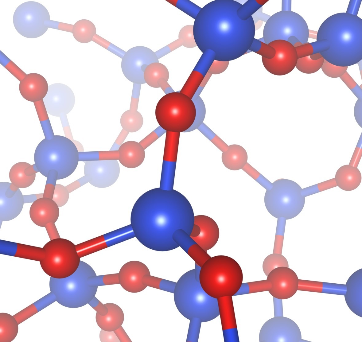
Under severe stress conditions, the breakage of atomic bonds can be the main reason for macroscopic power device malfunction.

Power semiconductor devices are commonly used for switching large loads in energy conversion systems, industrial applications, and other fields of daily life. However, the harsh environmental conditions and the extended operation ranges in such applications often pushes the classical semiconductor material Silicon to its physical limits. Due to their outstanding material properties, wide band gap materials such as Gallium Nitride (GaN) and Silicon Carbide (SiC) shift these physical limits to much higher values. Nevertheless, it is essential to understand the degradation mechanisms that occur under high-voltage, high-power, high-temperature, and/or high-current conditions. By the degradation under such circumstances along various paths, researchers eventually arrive at the smallest possible range, which is the atomic composition of the semiconductor material. Changes in the atomic structure of the materials that build up the device can alter the macroscopic performance, such as the threshold voltage or the drain current, and eventually lead to device failure. These atomic transitions, which impact the macroscopic behavior of the device, are commonly referred to microscopic defect creation and charging. Only a limited number of researchers have the opportunity to gain insights into such phenomena.
KAI Competences
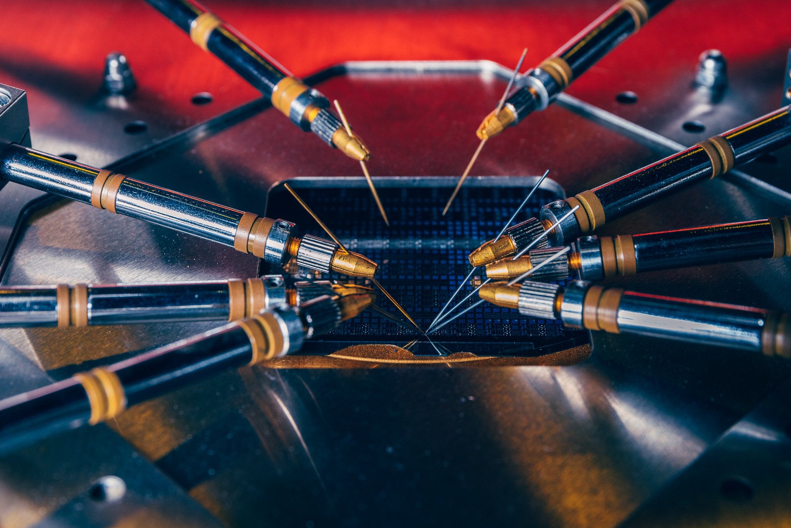
In recent years, KAI has established several electrical measurement and analysis approaches to understand the impact of microscopic defects on the performance and reliability of wide band gap devices. Some of the available approaches include electro-optical characterization methods such as charge pumping, impedance spectroscopy, deep level transient or optical spectroscopy (DLTS/DLOS), Hall measurements, and several others.


Electrical Characterization of Microscopic Defects
Exploring the composition and properties of microscopic defects is crucial in preventing future failures of power devices. In order to achieve this, researchers suggest microscopic defect models and validate these models through sophisticated electrical measurements on differently processed devices.
Semiconductor Device Physics Laboratory
Follow this link to read more about our Semiconductor Device Physics Laboratory.
